Introduction
Constructing a microphone array is a challenge of its own, but how do we actually process the microphone array data to do things like filtering and beamforming? One solution is to store the data on off-chip memory for later processing. This solution is great for experimenting with different microphone arrays since we can process the data offline and see what filter combinations work best from the data that we collected. This solution also avoids having to make changes to the hardware design any time we want to change filter coefficients or what algorithm is being implemented.
Overview of a basic microphone array system
Here’s a quick refresher of the DE1-SoC, the development board we use to process the microphone array.
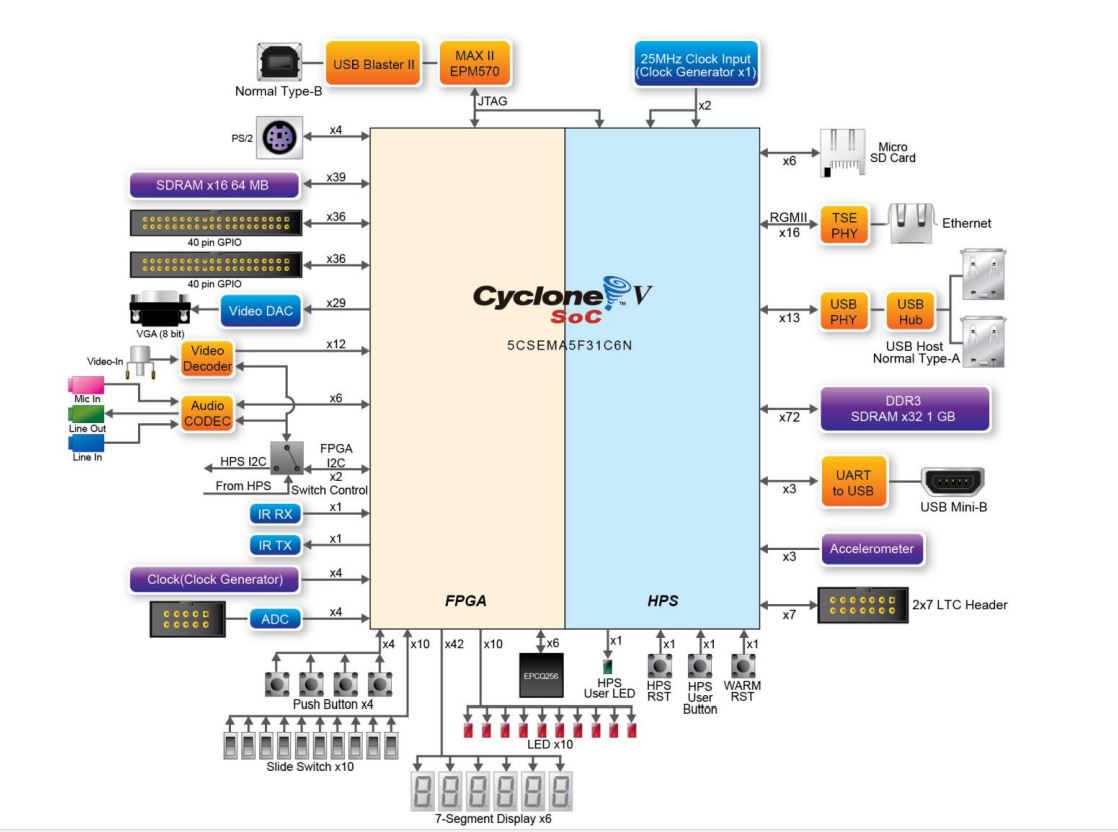
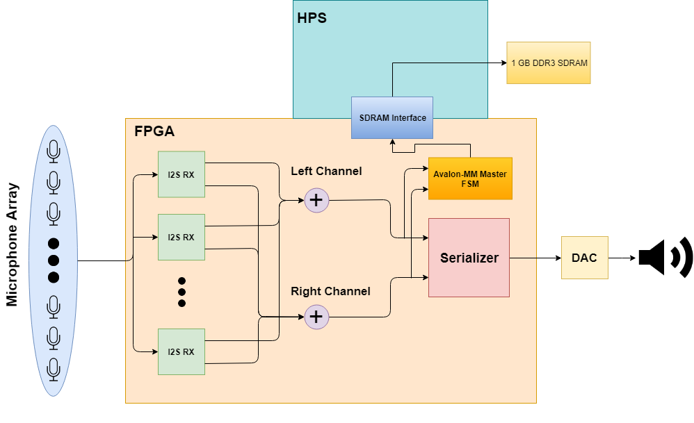
The main components in this project that we utilize are the GPIO pins, off-chip DDR3 memory, the HPS, and the Ethernet port. The microphone array connects to the GPIO port of the FPGA. The digital I2S data is interpreted on the FPGA by deserializing the data into samples. The 1-GB off-chip memory is where the samples will be stored for later processing. The HPS that is running linux will be able to grab the data from memory and store it on the SD card. Connecting the Ethernet port on a computer gives us the ability to grab the data from the FPGA seamlessly using shell and python scripts.
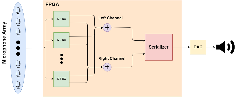
Currently the system is setup to stream the samples from the microphone array to the output of the audio codec. The microphones on the left side are summed up and output to the left channel, and the microphones on the right side are summed up and output to the right channel. The microphones are not processed before being sent to the CODEC. Here is a block diagram of what the system looks like before we add a DMA interface to the system.
How do we talk to off-chip memory?
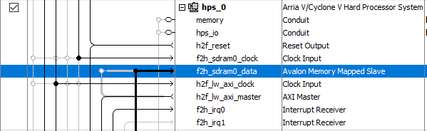
Taking a closer look at the picture of the Cyclone V, it should be noted that the off-chip DDR3 memory connects to the HPS on the DE1-SoC. This means that a traditional solution of writing code in verilog to talk to the pins of the off-chip memory will not suffice. Since only the HPS interacts with the off-chip memory the FPGA has to interact with the HPS to be able to store data to off-chip memory. This is what the block diagram looks like now.
What is the HPS?
The HPS is the hard processor system on-chip that’s on the Cyclone V. The Cyclone V is split in two parts: One part being the FPGA, and the other as a fully functional ARM-9 Cortex hard processor. The FPGA can communicate with the HPS back and forth using communication bridges that lie in the inter-fabric of the chip. Because the HPS can only interact directly with off-chip memory, we have to integrate the HPS into our project, further increasing the complexity for a DMA task. Fortunately this process is simplified by using the platform designer from Quartus to instantiate the IP to interface the HPS to our design.
SDRAM Memory Mapped Slave Port
In the platform designer we can specify that we want to add an interface to off-chip memory. This simplifies some of the process since we don’t have to create the interface itself, we just have to communicate to the interface based on the specified waveforms given be the IP.
FPGA-to-HPS SDRAM Interface
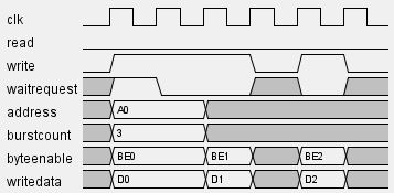
This interface is an Avalon Memory Mapped Slave. This means that the controller for the SDRAM is a slave, since it will listen for commands from the master that it is connected to. The interface to speak to the slave is done via memory mapped communication. Since the slave interface has a provided waveform of how it responds to signals from the master, we have to create our own Avalon Memory Mapped Master module to communicate to the SDRAM controller.
SDRAM slave write signal behavior

Master-Slave signals in action
The Avalon Memory Mapped Master will have a finite state machine in order to send the correct signals to the slave based on the state of the controller. The interface between the master and slave has six signals.

This picture is from the Master’s interface, it outputs five signals to tell the slave where in memory it should write, what data to write, and when to write the data. The input to the master is the wait signal from the slave. This signal tells us if the controller is busy and defines how our finite state machine will be designed based on the behavior of the wait signal.
The SDRAM Finite State Machine
Writing an FSM for writing to off-chip memory is where most of the challenge is since this component is responsible for sending data to memory. The first step is to have to have the implementation of writing a sample to memory working. Based on the waveform the AM_WAITREQUEST goes high one cycle after the AM_WRITE signal goes high. Then we wait for the AM_WAITREQUEST signal to go low. Once the AM_WAITREQUEST signal stays low this means that data was written to memory successfully.
This is simple enough to understand, but that is only for one sample. How do we stream samples from a single microphone channel to memory for a certain amount of time? There are a couple more signals that need to be introduced to do this. The first signal will tell us how many samples we want to store in memory. The microphone data is sampled at 48 kHz, so multiplying this value by the desired amount of time in seconds results in the total number of samples to be stored (e.g. 20 seconds of data => 48,000 * 20 = 960,000 samples). Now that we know how many samples we are storing, we can model the finite state machine to write for a certain amount of samples. The second signal we need is a signal to tell us when a new sample is ready. This signal will ensure that a sample is only written once to memory. Since the AM_WRITEDATA signal is 32 bits long and the microphone data is 16 bits we can store both channels in the AM_WRITEDATA signal. The last signal is the starting address signal. This signal will tell the controller where to start writing in memory. After every sample that is written to memory the address is incremented by 4 since a sample for both left and right channels are 4 bytes in length (32 bits). Here’s what the FSM for writing data from one microphone looks like.
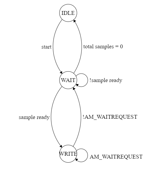
This FSM takes care of writing samples for one microphone, but in this project we have a microphone array, so we have to add more logic to the FSM to support recording for all of the microphones. This is done by cycling through all of the microphones when we see that a new sample is ready. Once the FSM writes all of the microphone samples to memory it waits for the next strobe of the new sample signal. Each microphone pair will write to a designated space in memory so that the samples do not get mixed up from all of the different channels. Here’s what is visually happening for storing data for 10 microphones.
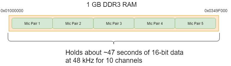
~47 Seconds of data.. That’s not a lot, what if I want more?
Right now with this iteration of the solution we have a functional FSM that handles writing data from a microphone array to off-chip memory. The next obstacle is figuring out how to work around the constraints of off-chip memory. We only have a finite amount of space to store data, and a good part of off-chip memory is reserved for the boot region and kernel space for the Linux OS running on the HPS. Through trial and error I found that the highest address I can write to without kernel panics is 0x0349F000. To work around this we can implement circular buffering to record data continuously without stepping out of bounds in memory.
Circular Buffering
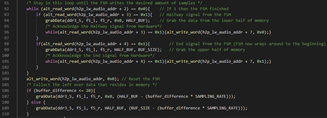
The idea here is that we setup buffers with enough space for 40 seconds worth of samples and once we write to the highest address we wrap around and continue writing starting from the beginning address again. There also needs to be additional logic added to the FSM so that the HPS grabs the data before the microphone data is overwritten from the FSM wrapping back around. To avoid this the FSM sends signals to the HPS when it reaches the halfway point in the buffer and at the end of the buffer. When the halfway signal is asserted the HPS stores the data from the beginning of the buffer to the address that’s halfway from the end. While the HPS is grabbing data the upper half of memory is being written with samples from the microphone array still. Once the FSM reaches the end and wraps around the end signal is asserted so that the HPS can grab the data from the halfway address to the last address in memory.
While the hardware is doing its part, the HPS needs to be ready to service the signals accordingly that are coming from the FSM. The HPS running Linux can run user programs written in C. Our audio program uses the memory map system call to map the region of memory where we write to in hardware to the user space in the audio program. Once the FSM starts writing to memory, the audio program polls the two signals from hardware and handles the signals by storing the data from that region of memory into a file. Once the FSM finishes writing to memory the data files are ready to be processed offline!