Using Notch for Low-Cost Motion Capture

This semester, I was fortunate to be able to toy around with a six-pack of Notch sensors and do some basic motion capture. Later in the semester, I was asked to do a basic comparison of existing motion capture technology that could be used for the tracking of microphone arrays.

Motion capture is necessary for certain projects in our lab because allows us to track the positions of multiple microphones in 3D space. When recording audio, the locations of the microphones are usually fixed, with known values for the difference in position. This known value allows us to determine the relative location of an audio source using triangulation.

For a moving microphone array, the position of each microphone (and the space between them) must be known in order to do correct localization calculations. Currently, our project lead Ryan Corey is using an ultrasonic localization system which requires heavy computing power and is not always accurate.

This segment of my projects is dedicated to determining the effectiveness of Notch for future use in the lab.

Continue reading

Constructing Microphone Arrays

Microphone arrays are powerful listening and recording devices composed of many individual microphones operating together in tandem. Many popular microphone arrays (such as the one found in the Amazon Echo) are arranged circularly, but they can be in any configuration the designer chooses. In our Augmented Listening Lab, we strive to make these arrays wearable to assist the hard of hearing or to serve recording needs. Over the past year, I have been constructing functional prototypes of microphone arrays using MEMS microphones and FPGAs.

Above is a MEMS microphone breakout board created by Adafruit. You can find it here: https://www.adafruit.com/product/3421

When placing these microphones into an array, they all share the Bit Clock, Left/Right Clock, 3V and Ground signals. All of the microphones share the same clock! Pairs of microphones share one Data Out line that goes to our array processing unit (in our lab we use an FPGA) and the Select pin distinguishes left and right channels for each pair.

The first microphone array I constructed was using a construction helmet! The best microphone arrays leverage spatial area – the larger area the microphones surround or cover, the clearer the audio is. Sometimes in our lab, we test audio using microphone arrays placed on sombreros – a wide and spacious area. Another characteristic of good microphone array design is spacing the microphones evenly around the area. The construction helmet array I built had 12 microphones spaced around the outside on standoffs and I kept the wires on the inside.

Finally, we use a Field Programmable Gate Array (FPGA) to do real time processing on these microphone arrays. SystemVerilog makes it easy to build modules that control microphone pairs and channels. FPGAs are best used in situations where performance needs to be maximized, in this case we need to reduce latency as much as possible. In SystemVerilog we can build software for our specific application and declare the necessary constraints to make our array as responsive and efficient as possible.

My next goal was to create a microphone array prototype thats wearable and has greater aesthetic appeal than the construction helmet. My colleague, Uriah, designed a pair of black, over-the-ear headphones that contain up to 11 MEMS microphones. The first iteration of this design was breadboarded but future iterations will be cleaned up with a neat PCB design.

A pic of me wearing the breadboarded, over-the-ear headphone array.

Tutorial 1: Simple Accumulator

Introduction

In this first tutorial we will create a design that will be able to increment or decrement a value by pushing buttons on the FPGA and displaying the hex value on the hex display on the board. This will cover combinational logic design, sequential logic design, and how to interface some of the peripherals on the FPGA as well as loading the design on the board.

Sequential vs parallel programming languages

Solving this problem with a microprocessor that executes instructions sequentially (like an Arduino) is pretty trivial to do. The code might look something like this…

/* PSEUDO CODE (will not compile on Arduino's IDE) */
while(1){
   if (button1){
      accumulator = accumulator + 1;
      while (button1) {}
   } else if (button2){
      accumulator = accumulator - 1;
      while (button2) {}
   }
}

Solving this problem in a hardware description language might not be so obvious. In SystemVerilog we are describing a digital circuit that will execute code in parallel. In order to achieve the same functionality as the sequential code from above we have to create a combinational and sequential logic circuit.

What is a combinational logic circuit?

A combinational logic circuit has a defined output based on all different combinations of its inputs – it’s kind of similar to a math function. Let’s consider an example of a familiar math function: f(x) = x^2. This function always has an output for any real value that is fed to this function: f(0) = 0, f(2) = 4, f(3) = 9, f(3.14159) = 9.8690, etc. In the digital world we can also have functions like this, but our inputs and outputs either have the value of 0 or 1. These functions are called boolean functions, and they are made up logic gates like AND, OR, NOT, NAND, etc. The link below covers the functionality of these logic gates with diagrams and truth tables.

http://www.ee.surrey.ac.uk/Projects/CAL/digital-logic/gatesfunc/

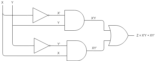
We can piece these logic gates together to create a combinational logic circuit and represent it with a function. Let’s create an XOR (exclusive or) circuit using AND, OR, and NOT gates. We will first create a truth table for XOR.

x  y | z
-------
0  0 | 0
0  1 | 1
1  0 | 1
1  1 | 0

This function’s output is 1 when X is 0 and Y is 1 (X’Y), OR when X is 1 and Y is 0 (XY’). If they are both 1 or both 0 the output is 0. We can write this function as z = x’y + xy’. The concatenation of two variables ‘xy’ represents the AND operation, the ‘ represents the NOT operation, and the ‘+’ represents the OR operation. Our combinational circuit looks like this.

That’s pretty neat, but how do we apply this to the problem we are trying to solve?

So now we know how to create a logic circuit, but how would we make a circuit that can increment and decrement a variable? We can start to think of what our inputs to this circuit would be: two different buttons on the FPGA – where one button will be the signal to increment and the other to decrement. We also need to think about how we can create something like a variable in hardware and how we can control what values it takes on. More specifically, we need to be able to have a way where we can remember what value our accumulator had and how our inputs to this circuit can control what values it takes on. To accomplish this we have to understand how sequential logic works.

What is sequential logic?

* Fill in detailed description *

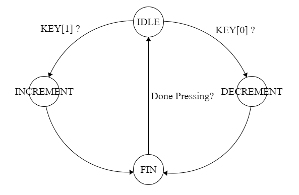
Finite state machine design

Transferring your design into functional code

https://github.com/juanjm2/I-Vault-Blog-Code/tree/master/Tutorial_1

Quartus Tutorial

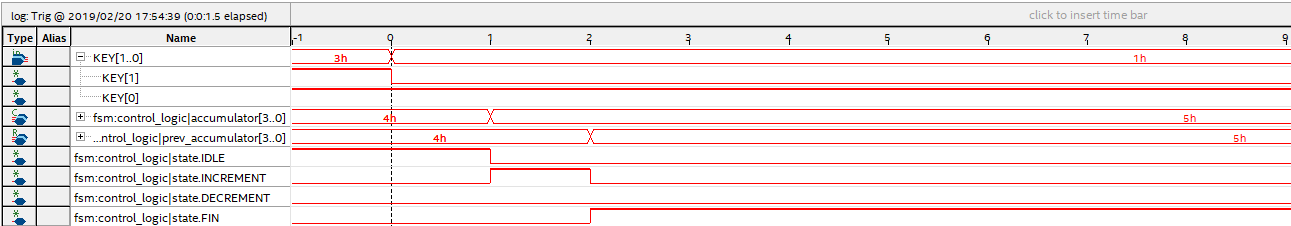
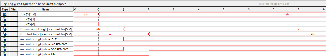
Actual FSM Behavior in hardware