Introduction
In this first tutorial we will create a design that will be able to increment or decrement a value by pushing buttons on the FPGA and displaying the hex value on the hex display on the board. This will cover combinational logic design, sequential logic design, and how to interface some of the peripherals on the FPGA as well as loading the design on the board.
Sequential vs parallel programming languages
Solving this problem with a microprocessor that executes instructions sequentially (like an Arduino) is pretty trivial to do. The code might look something like this…
/* PSEUDO CODE (will not compile on Arduino's IDE) */
while(1){
   if (button1){
      accumulator = accumulator + 1;
      while (button1) {}
   } else if (button2){
      accumulator = accumulator - 1;
      while (button2) {}
   }
}
Solving this problem in a hardware description language might not be so obvious. In SystemVerilog we are describing a digital circuit that will execute code in parallel. In order to achieve the same functionality as the sequential code from above we have to create a combinational and sequential logic circuit.
What is a combinational logic circuit?
A combinational logic circuit has a defined output based on all different combinations of its inputs – it’s kind of similar to a math function. Let’s consider an example of a familiar math function: f(x) = x^2. This function always has an output for any real value that is fed to this function: f(0) = 0, f(2) = 4, f(3) = 9, f(3.14159) = 9.8690, etc. In the digital world we can also have functions like this, but our inputs and outputs either have the value of 0 or 1. These functions are called boolean functions, and they are made up logic gates like AND, OR, NOT, NAND, etc. The link below covers the functionality of these logic gates with diagrams and truth tables.
http://www.ee.surrey.ac.uk/Projects/CAL/digital-logic/gatesfunc/
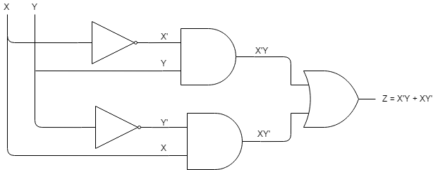
We can piece these logic gates together to create a combinational logic circuit and represent it with a function. Let’s create an XOR (exclusive or) circuit using AND, OR, and NOT gates. We will first create a truth table for XOR.
x  y | z
-------
0  0 | 0
0  1 | 1
1  0 | 1
1  1 | 0
This function’s output is 1 when X is 0 and Y is 1 (X’Y), OR when X is 1 and Y is 0 (XY’). If they are both 1 or both 0 the output is 0. We can write this function as z = x’y + xy’. The concatenation of two variables ‘xy’ represents the AND operation, the ‘ represents the NOT operation, and the ‘+’ represents the OR operation. Our combinational circuit looks like this.
That’s pretty neat, but how do we apply this to the problem we are trying to solve?
So now we know how to create a logic circuit, but how would we make a circuit that can increment and decrement a variable? We can start to think of what our inputs to this circuit would be: two different buttons on the FPGA – where one button will be the signal to increment and the other to decrement. We also need to think about how we can create something like a variable in hardware and how we can control what values it takes on. More specifically, we need to be able to have a way where we can remember what value our accumulator had and how our inputs to this circuit can control what values it takes on. To accomplish this we have to understand how sequential logic works.
What is sequential logic?
* Fill in detailed description *
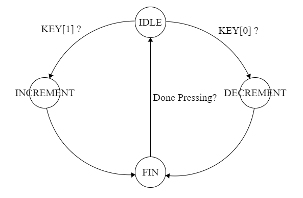
Finite state machine design
Transferring your design into functional code
https://github.com/juanjm2/I-Vault-Blog-Code/tree/master/Tutorial_1
Quartus Tutorial
Actual FSM Behavior in hardware


