At the 2023 CS MANTECH conference, Kevin presents his work on using anti-phase coatings to achieve high-power, single-mode performance in VCSELs.
Category: Publications
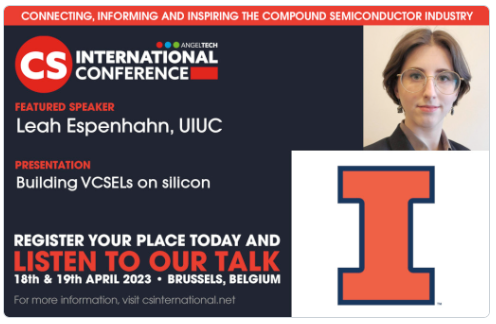
Leah Presents Integration Work at CS International
At the 2023 CS International Conference in Brussels, Belgium, Leah gave an invited talk on her work making heterogeneously integrated VCSELs on silicon. These VCSELs integrated via epitaxial transfer have improved thermal performances compared to non-integrated counterparts.
Robert, Kevin, and Leah Present at the Engineering Research Fair
Robert Kaufman, Kevin Pikul, and Leah Espenhahn present a high-level view on the research conducted within the group at the 2023 Engineering Research Fair. Over the course of two hours, 74 undergraduate students show interest in the group and the research being performed.
Laser Islands: Illinois Researcher Leah Espenhahn Shows How to Fully Integrate VCSELs on Silicon
Leah Espenhahn, Kevin Pikul, and Prof. Dallesasse are interviewed about their article published in Compound Semiconductor. They explore the topics of VCSELs and III-V/Si integration via epitaxial transfer.
Compound Semiconductor Article

Achieving high-power single-mode operation in vertical-cavity surface-emitting lasers via scalable, higher-order mode suppression techniques
Achieving high-power single-mode operation in Vertical-Cavity Surface-Emitting Lasers (VCSELs) has received renewed interest due to performance needs driven by facial recognition and 3D imaging in mobile telephones. Two distinct mode control methods that rely on exploiting the spatial field distribution of optical transverse modes to achieve high-power single-mode operation in VCSELs will be discussed. The first method uses a surface-deposited optical coating of multilayer SiO2/TiO2 or single-layer silicon to achieve single-mode emission. The capability to pattern these layers in a wafer-scale process makes this method attractive for high-volume manufacturing. The second method utilizes impurity-induced layer disordering (IID) to selectively intermix the top distributed Bragg reflector (DBR) in a VCSEL, thereby creating a mirror whose reflectivity spatially varies across the aperture. Using these techniques, single-mode output power in excess of 10 mW has been demonstrated with side-mode suppression ratios in excess of 35 db.
Impact of Diffusion Profile on the Modulation Response of Single-Mode Disorder-Defined VCSELs
The impact of diffusion profile shaping through the use of tensilely and compressively strained diffusion masks on the modulation response of single-mode vertical-cavity surface-emitting lasers (VCSELs) using disorder-defined apertures is investigated. VCSELs designed for high-power single-fundamental-mode emission through the use apertures defined via impurity-induced disordering (IID) in conjunction with a standard oxide-confinement process are characterized to extract high-frequency optical cavity parameters across oxide aperture and diffusion mask strain variations. The 3-dB small-signal bandwidth is maintained for a 7.68 mW single-mode 850 nm VCSEL with an oxide aperture of 13 μm using a tensilely strained diffusion mask relative to a non-disordered multimode device of the same oxide aperture. A large K-factor reduction is also observed, from 0.248 ns to 0.045 ns, indicating that damping and photon lifetimes within the cavity of VCSELs employing disorder-defined apertures are substantially reduced. Performance implications to data communication applications are discussed.
IEEE Photonics Technology Letters Article Link
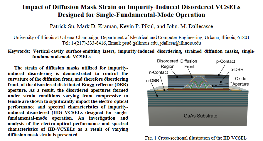
Impact of Diffusion Mask Strain on Impurity-Induced Disordered VCSELs Designed for Single-Fundamental-Mode Operation
The strain of diffusion masks utilized for impurity-induced disordering is demonstrated to control the curvature of the diffusion front, and therefore disordering front, of the disordered distributed Bragg reflector (DBR) aperture. As a result, the disordered apertures formed under strain conditions varying from compressive to tensile are shown to significantly impact the electro-optical performance and spectral characteristics of impurity-induced disordered (IID) VCSELs designed for single-fundamental-mode operation. An investigation and analysis of the electro-optical performance and spectral characteristics of IID-VCSELs as a result of varying diffusion mask strain is presented.
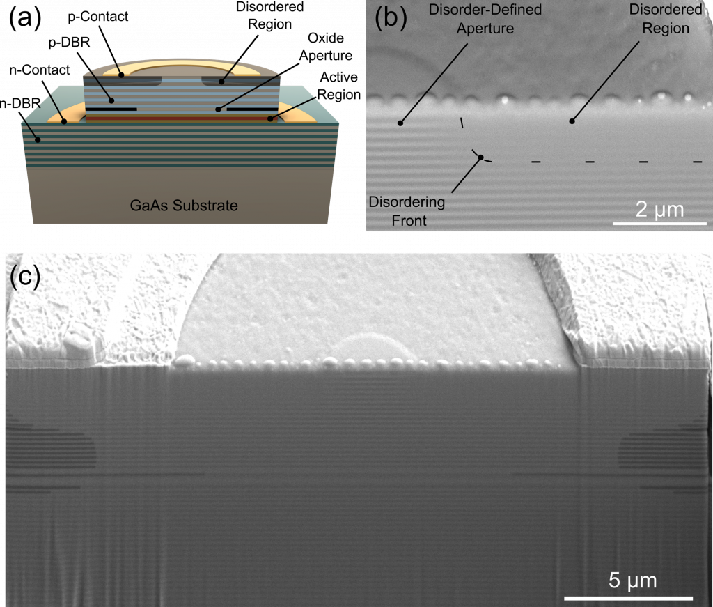
Heterogeneously integrated VCSELs on silicon
A wafer-scale CMOS-compatible process for heterogeneous integration of III-V epitaxial material onto silicon for photonic device fabrication is presented. Transfer of AlGaAs-GaAs Vertical-Cavity Surface-Emitting Laser (VCSEL) epitaxial material onto silicon using a carrier wafer process and metallic bonding is used to form III-V islands which are subsequently processed into VCSELs. The transfer process begins with the bonding of III-V wafer pieces epitaxy-down on a carrier wafer using a temporary bonding material. Following substrate removal, precisely-located islands of material are formed using photolithography and dry etching. These islands are bonded onto a silicon host wafer using a thin-film non-gold metal bonding process and the transfer wafer is removed. Following the bonding of the epitaxial islands onto the silicon wafer, standard processing methods are used to form VCSELs with non-gold contacts. The removal of the GaAs substrate prior to bonding provides an improved thermal pathway which leads to a reduction in wavelength shift with output power under continuous-wave (CW) excitation. Unlike prior work in which fullyfabricated VCSELs are flip-chip bonded to silicon, all photonic device processing takes place after the epitaxial transfer process. The electrical and optical performance of heterogeneously integrated 850nm GaAs VCSELs on silicon is compared to their as-grown counterparts. The demonstrated method creates the potential for the integration of III-V photonic devices with silicon CMOS, including CMOS imaging arrays. Such devices could have use in applications ranging from 3D imaging to LiDAR.
Kevin Pikul Awarded Best Student Presentation Award of CS MANTECH 2021
Kevin Pikul is awarded the best student presentation award of CS MANTECH 2021 based on his paper titled “Standing-Wave Engineering for Mode-Control in Oxide-Confined Vertical-Cavity Surface-Emitting Lasers”.


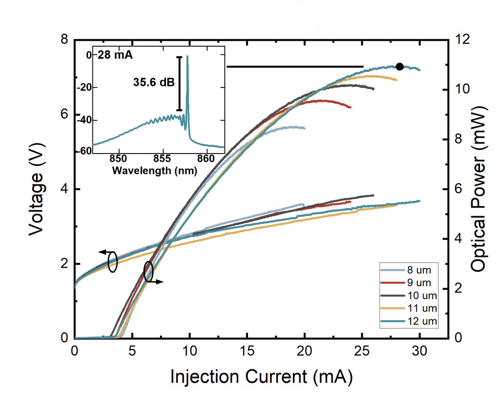
Record High-Power Single-Mode VCSELs using Strain-Controlled Impurity-Induced Disordering Apertures
Patrick Su demonstrates record high-power single-mode performance in VCSELs using strain-controlled impurity-induced disordering apertures. Oxide-VCSELs of aperture sizes from 9-13 um are shown to achieve record single-mode output powers of 8.52 mW, 9.57 mW, 10.20 mW, 10.57 mW, and 10.95 mW respectively.
Applied Physics Letter Article Link