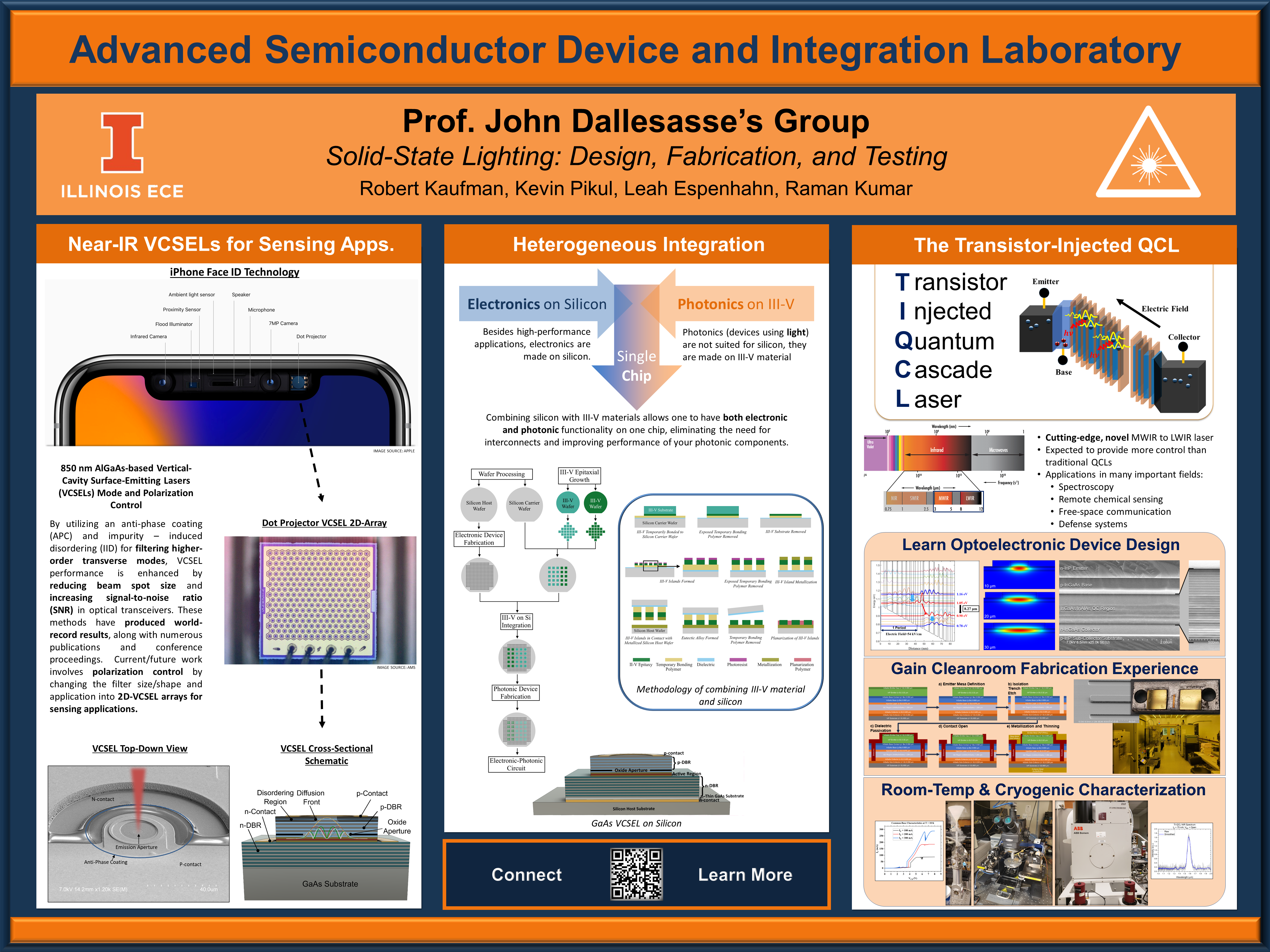
Robert Kaufman, Kevin Pikul, and Leah Espenhahn present a high-level view on the research conducted within the group at the 2023 Engineering Research Fair. Over the course of two hours, 74 undergraduate students show interest in the group and the research being performed.
Leah Espenhahn, Kevin Pikul, and Prof. Dallesasse are interviewed about their article published in Compound Semiconductor. They explore the topics of VCSELs and III-V/Si integration via epitaxial transfer.
A wafer-scale CMOS-compatible process for heterogeneous integration of III-V epitaxial material onto silicon for photonic device fabrication is presented. Transfer of AlGaAs-GaAs Vertical-Cavity Surface-Emitting Laser (VCSEL) epitaxial material onto silicon using a carrier wafer process and metallic bonding is used to form III-V islands which are subsequently processed into VCSELs. The transfer process begins with the bonding of III-V wafer pieces epitaxy-down on a carrier wafer using a temporary bonding material. Following substrate removal, precisely-located islands of material are formed using photolithography and dry etching. These islands are bonded onto a silicon host wafer using a thin-film non-gold metal bonding process and the transfer wafer is removed. Following the bonding of the epitaxial islands onto the silicon wafer, standard processing methods are used to form VCSELs with non-gold contacts. The removal of the GaAs substrate prior to bonding provides an improved thermal pathway which leads to a reduction in wavelength shift with output power under continuous-wave (CW) excitation. Unlike prior work in which fullyfabricated VCSELs are flip-chip bonded to silicon, all photonic device processing takes place after the epitaxial transfer process. The electrical and optical performance of heterogeneously integrated 850nm GaAs VCSELs on silicon is compared to their as-grown counterparts. The demonstrated method creates the potential for the integration of III-V photonic devices with silicon CMOS, including CMOS imaging arrays. Such devices could have use in applications ranging from 3D imaging to LiDAR.
The promise of silicon integrated circuits with their electronic or photonic functionality enhanced via heterogeneous integration has motivated significant work in understanding and overcoming the barriers to realizing such an IC. Additional hurdles must be overcome when integrating devices that are highly sensitive to temperature variation such as semiconductor lasers. Challenges in the heterogeneous integration process will be reviewed, and approaches for heterogeneous integration that have the potential to enable silicon ICs with enhanced functionality will be discussed in the context of integrated photonic systems.
At the International Compound Semiconductor Manufacturing Technology (CS MANTECH) 2018, John Carlson and Patrick Su were honored with the Best Poster Award on a method of integrating III-V semiconductor material suitable for lasers onto silicon which is used for CMOS electronics. John has demonstrated a novel demonstration of epitaxial bonding and transfer for heterogeneous integration of electron-photonic circuitry.