Skip to content
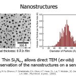 Using very thin (15-30 nm) nitride in our sensors allows us to deposit our sample and move the sensor into a TEM with no further sample preparation.
- This micrograph shows the particles that form on nitride form an 8 Å In deposition.
- We then digitize these images and use a series of image analysis techniques to determine a distribution of particle sizes.
 Nanoscale materials do not behave as our macro-world experiences tell us they should.
- In nanoparticles a significant fraction of the atoms are at the surface and surface effects can dominate.
- Here one can see indium particles melt at temperatures far below that of bulk indium. At 1 nm, they can even be liquid at room temperature.
- ΔTm proportional to (1/r).
- ΔHm drops also (although not shown here).
- We have a distribution of particle sizes, which means an ensemble of particles will not have a single, well-defined melting temperature, but a broad peak.
- e found multiple, discrete melting points. We can determine the size of the particle that corresponds to each peak from the Tm depression. The red line shows particles of about 70 Å melting; the blue line shows particles of 20 Å melting.
- The peaks are not spaced at regular temperature intervals.

- Melting temperature is a non-linear function of particle radius.
- The peaks are separated by the thickness of a monolayer.
- We attribute this to the magic number effect. Particles with an incomplete shell of atoms are energetically less favorable than particles with a complete shell.
- It can be seen that the sizes of the particles at the Tm peaks correlate well with the atomic magic numbers calculated from theory.